
We manufacture
electronics.
EMS · Berlin · since 1991
From your data to tested production: SHK manufactures and assembles complex electronic assemblies — built to the highest quality standards. Where production data needs adjusting for manufacturability, we support you.

Capabilities: EMS, subcontracting, hybrid manufacturing


EMS
The full service. We source the components on the best terms, manufacture your assembly and, on request, test it electrically. From the layout phase onward we design for manufacturability and testability — avoiding costly corrections later. If needed, our test engineer creates the complete test concept, including test fixtures and software.
Subcontracting
You supply the components and circuit boards, we handle the manufacturing. The dependable option when procurement and material planning stay on your side and you need pure production capacity — with the same quality assurance and traceability as our full EMS service.
Hybrid manufacturing
Our specialty since 1991: customer-specific thick-film circuits on ceramic substrate. Conductors and resistors are screen-printed, fired at around 800 °C and laser-trimmed to better than 0.1 %. Robust against high temperatures, allowing highly miniaturised designs and suitable for high-voltage applications up to 30 kV.
One technology spectrum,
one depth of manufacturing.
As an EMS provider we cover the full range of electronic assembly and interconnection technology — from the finest SMD packages to customer-specific thick-film hybrid circuits.
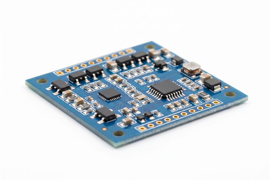
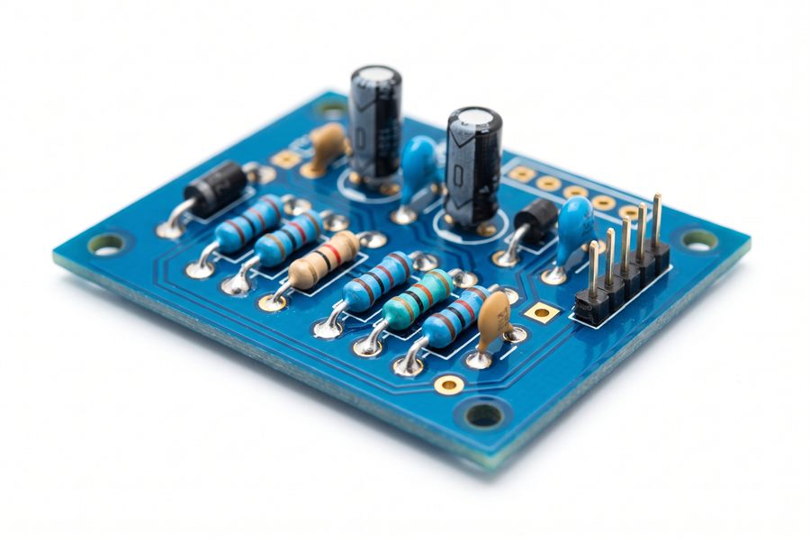
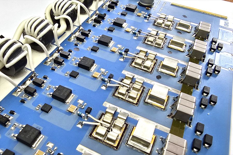
Machines that make precision possible.
Our lines combine established systems from leading manufacturers — from stencil printing through component placement to automated optical inspection.

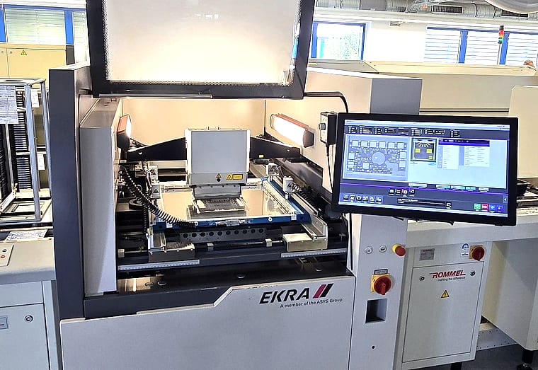
Stencil printing
Solder paste deposition is the first and most quality-critical step of every SMD assembly. All lines run the same EKRA printer — reproducible regardless of the line. The integrated 2.5D paste inspection checks every print for volume and height, detects bridging and clogged stencil apertures, and corrects the process before placement begins.
SMD placement
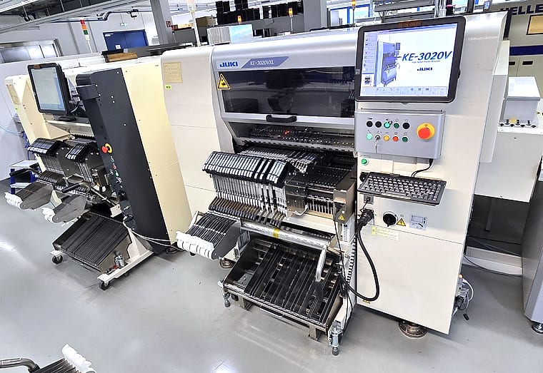
Placement runs exclusively on JUKI machines — from the FX-3 and RX-6 high-speed mounters for large volumes to the flexible RE-2060 and KE-3020V systems for complex, mixed assemblies. That covers everything from 01005 chips to large ICs, connectors and odd-form parts — laser and vision centring capture every component individually, fine-pitch, BGA and µBGA included.
AOI
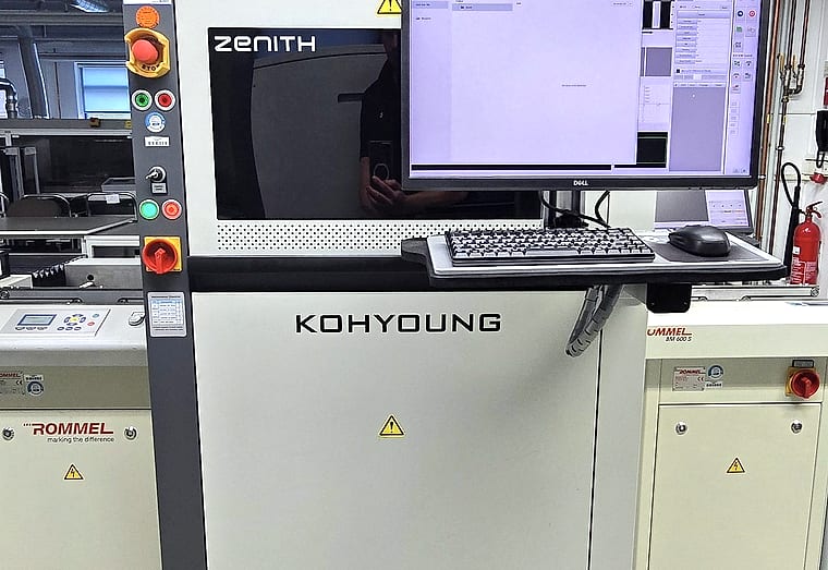
After soldering, automated optical inspection checks every solder joint and component — measured in 3D rather than merely compared. The Koh Young and Viscom systems reliably detect solder defects, missing or reverse-polarity parts and offset before the assembly leaves the line.
Selective soldering
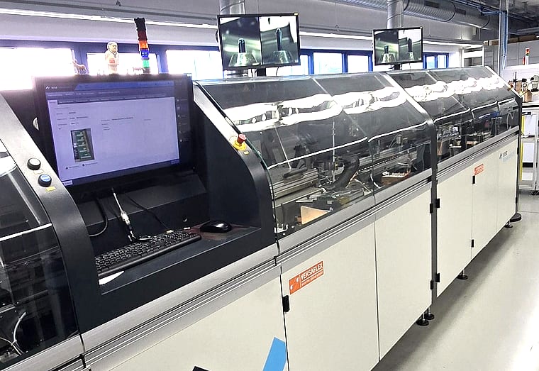
For through-hole components, the Ersa selective soldering system solders each joint individually and on target — with low thermal load, ideal for dense or heat-sensitive assemblies. Soldering runs under nitrogen for clean, oxidation-free joints.
Wave soldering
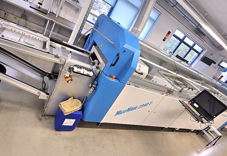
For higher volumes, the enclosed SEHO nitrogen wave soldering system takes over: the assembly passes a standing solder wave that joins all leaded connections in a single pass. The nitrogen enclosure keeps the joints oxidation-free.
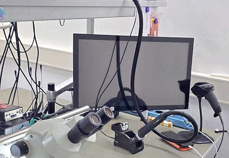
Hand soldering & rework
At microscope workstations with JBC soldering equipment we handle manual soldering, rework and repairs — from a single correction to component replacement on the finest packages. Prototypes and very small batches are built here under magnification too.
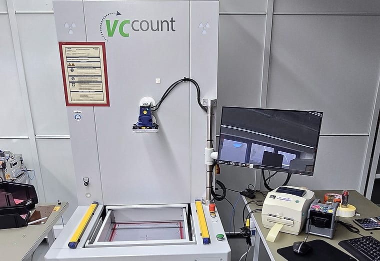
X-ray counting system
At goods-in, an X-ray system counts components in reels, trays and tubes — without unwinding or opening them. This ensures accurate stock levels and reliable material planning from the very first minute.
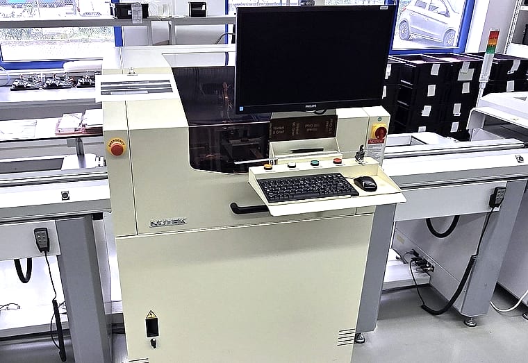
Laser marking
The Nutek laser marks every assembly permanently and tamper-proof — with plain text, barcode or Data Matrix code directly onto the substrate or onto an applied heat-resistant label. This is the basis for seamless traceability from the very first production step.
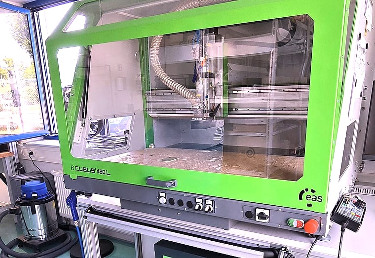
In-house tooling
Two CNC mills and two 3D printers produce carriers, soldering frames and test fixtures on site. We optimise production data such as solder-paste stencils ourselves via CAM software — short paths, fast iteration, a continuously improving process.
From idea to tested production.
Idea & consulting
Technology consulting by our engineers, component sourcing on the best terms.
Data check & DFM
Review of your production data, design for manufacturability and testability.
Placement
SMD and THT assembly on modern automated lines.
AOI
Optical inspection of solder joints after reflow and wave soldering.
Electrical testing
Functional testing to customer specification, including test fixtures and software.
Production
Small, medium and large series — traceable and reproducible.
Certified,
audited, traceable.
All manufacturing processes are defined and certified under a quality management system to DIN EN ISO 9001. ESD-protected production areas, climate-controlled printing processes and a closed ventilation system ensure consistent quality — checked in-process by visual inspection and AOI after reflow soldering.
We manufacture for customers in medical technology and the automotive industry, among others, and have been successfully audited by individual customers from these sectors. Two of our automated lines run a traceability system from Cogiscan: seamless traceability of material and process data per assembly.

Let's talk about your assembly.
Send us your enquiry — our engineers will advise you from the first feasibility question through to series production.
Or by e-mail:
For a quick assessment, a bill of materials (BOM) and Gerber files are enough to start.